Key Takeaway:
3D CT scans through a component layer by layer, revealing sub-surface cracks, voids, and bond defects that 2D X-ray often misses. Catching these issues before overmolding is far cheaper than catching them after, since defective units can still be reworked or scrapped before final encapsulation. Typical finds include wire bond lift-off, die attach voids, micro-cracks, and underfill voids. Malaysian firms work with Singapore-based labs like PTSPL for the higher resolution, faster turnaround, and ISO/IEC 17025:2017 backing.
Table of Contents
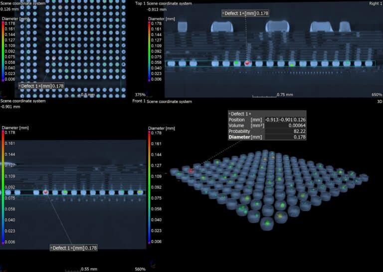
In semiconductor manufacturing, a sub-surface void or micro-crack in a solder joint or wire bond can mean millions in scrap costs, especially when it surfaces after final overmolding. By that stage, rework is rarely an option, and the part either fails on the test bench or, worse, in the customer’s hands. It’s imperative to catch those defects before they’re sealed into the package, and this is where 3D CT shines.
If you’re a Malaysian semiconductor firm, let’s walk you through how X-ray inspection for electronic components using 3D CT helps you detect defects before they become costly failures, and what to look for when scoping a CT inspection programme.
Why 3D CT for Semiconductors?
Compared to a 2D X-ray, which gives a flat shadow image of a component, 3D CT scanning for semiconductors goes further by reconstructing the part as a full volume, then “slicing” through it digitally at any plane the user needs. This comes with several advantages:
- Detects sub-surface cracks, voids, delamination, wire bond defects, and die attach issues
- Non-destructive, so the same component can be inspected, returned to production, or sent for further testing
- High resolution suitable for the micro-scale features inside chips and packages
- Applicable at almost any stage of the semiconductor fabrication process, from incoming material checks to final QA
The 3D dataset also opens up applications that sit close to semiconductor metrology in concept, such as void volume quantification in solder joints or dimensional verification of bond geometry.
The ROI Argument: Catch Defects Before Overmolding
The economics here are simple. The earlier a defect is caught, the less it costs to deal with.
Pre-Mold vs Post-Mold Detection
- Defect found before overmolding → Rework, rebond, or scrap individual units at minimal cost
- Defect found after overmolding → Entire batch may need to be scrapped; rework is often impossible
- Defect found at the customer end → Returns, warranty claims, reputation damage, and potential recalls
The stakes are especially high for AI chips, as you are also contending with high unit value, tight yield margins, urgent turnaround windows, and customer expectations of zero-defect shipments. A single defective device shipped to an OEM costs you both the part and a measure of trust with that customer.
Beyond Scrap Savings
- CT data supports proper root cause analysis, allowing fixes at the process level rather than just the part level
- Strengthens supplier accountability when incoming components are the source of the problem
- Detailed CT inspection reports help demonstrate rigorous QA practices to OEMs and end-clients
For high-value, low-volume production, new product introduction, supplier qualification, and post-failure investigation, an industrial CT scan for semiconductors typically pays for itself with a handful of caught defects.
Common Defects 3D CT Detects in Semiconductor Components
- Wire bond defects: lift-off, sagging, broken wires, or inconsistent loop height that affect electrical connectivity and long-term reliability
- Die attach issues: voids, insufficient coverage, or delamination in the adhesive layer that compromise thermal dissipation and mechanical stability
- Die tilt or misalignment: positioning errors that affect wire bonding accuracy and downstream assembly steps
- Substrate and die cracks: micro-fractures from handling, thermal stress, or process issues, which can propagate under operating conditions
- Underfill voids: air pockets in the encapsulant that reduce mechanical support and create stress concentration points
- Foreign particle contamination: debris trapped during assembly, with the potential to cause short circuits or reliability failures
Why Malaysian Firms Use Singapore Labs
Most retest delays are avoidable with better planning at the front end. Here are a few practical steps to take:
- Confirm test requirements upfront, including temperature, orientation, and number of specimens
- Talk to the lab before testing if any part of the spec is unclear
- For welds, make sure the procedure qualification reflects production conditions accurately
- If a failure does occur, consult the lab on root cause analysis before committing to a retest
How PTSPL Handles 3D CT Inspection
Phase 1: Scoping and Agreement
- Consultation and NDA: We sign a non-disclosure agreement before any proprietary details about samples or projects are shared
- Scope of work and quotation: tests, methods, and acceptance criteria are defined, and a formal quote is issued based on the agreed scope
- Commercial agreement: terms, payment conditions, and client onboarding are finalised
Phase 2: Sample Handling and Testing
- Sample submission: clients ship samples directly or use our delivery services. All materials receive a unique tracking ID for end-to-end traceability per ISO standards
- CT scanning and analysis: computed tomography is performed against the agreed scope, followed by evaluation against the client’s acceptance criteria
Phase 3: Review and Delivery
- QC and validation: Our internal team validates results against acceptance criteria and quality standards for accuracy and repeatability
- Preliminary review: We collaborate with you on initial findings, fine-tuning testing parameters where needed to align with project goals
- Final report and data handoff: You receive the complete CT data package, including raw scan files (DICOM, TIFF stacks, or other agreed formats), technical documentation, and the final report. Data is delivered securely via encrypted cloud transfer or physical drive
- Post-service support: our team remains available for technical questions, ensuring full clarity on the data before final invoicing
Protect Your Yield with PTSPL's 3D CT Services
For players in Malaysia’s semiconductor supply chain, 3D CT scanning and inspection is a cost-saving investment that allows you to catch defects before final overmolding. Though there’s the cost of the scan itself, this helps protect your margins, customer relationships, and the project schedule, which matter even more in AI-grade and high-reliability applications.
If you’re in need of industrial CT scanning for semiconductors, PTSPL operates as an independent testing laboratory across Singapore, Malaysia, and Indonesia, with ISO/IEC 17025:2017 accreditation through SAC-SINGLAS, DSM, and KAN, respectively. Our 3D CT capability is supported by experienced technical staff who work closely with semiconductor clients on defect analysis, supplier qualification, and root cause investigations.
Frequently Asked Questions About 3D CT for Semiconductor Inspection
2D X-ray produces a single flat shadow image of a component, which can hide overlapping features and small sub-surface defects. 3D CT reconstructs the entire part as a digital volume, allowing the user to slice through any plane and isolate features such as voids, micro-cracks, and bond defects in three dimensions. For complex packages, that depth of view is what makes the difference between a clear pass and a missed defect.
Yes, since the technique is non-destructive and X-rays penetrate most encapsulant materials. That said, the value of CT increases significantly when used before overmolding, when defective units can still be reworked or scrapped at minimal cost. Post-mold CT is most often used for failure analysis, customer return investigations, and supplier accountability cases.
Turnaround depends on sample volume, scan resolution, and reporting requirements, but most projects move significantly faster than shipping samples to the US or Europe. PTSPL works with Malaysian clients on logistics, scoping, and prioritisation, and urgent or pre-shipment inspection scenarios are typically accommodated with prior coordination.
CONTACT PTSPL TODAY
Explore our X-ray inspection for electronic components using industrial 3D CT, backed by responsive technical support throughout. Get in touch with us today to discuss your inspection requirements.