Key Takeaway:
- Budget USB-C cables often lack shielding, use fewer copper wires, and have weak solder joints. These flaws are invisible to the naked eye but clearly revealed through X-ray CT scanning.
- Premium USB-C cables (e.g., Apple Thunderbolt 4) feature multi-layer shielding, dedicated PCBAs, full pin counts, and reinforced strain relief designs.
- 3D X-ray computed tomography creates detailed volumetric models of cable interiors, allowing engineers to inspect solder quality, wire density, and structural integrity without cutting anything open.
- CT scanning has practical applications beyond consumer electronics, supporting failure analysis, prototype validation, supplier QC, and product design verification across industries.
Table of Contents
USB-C cables are everywhere, from consumer electronics to industrial equipment, yet despite their universal connector shape, their internal construction varies enormously. Two cables that look identical on the outside can deliver completely different levels of performance and durability, and there’s no way to tell which is which from the packaging alone.
The difference lies in what’s hidden beneath the outer jacket: the wiring, solder joints, shielding layers, and strain-relief design. These are the factors that determine why USB-C cables break prematurely or why do USB-C cables stop working after just a few months of regular use.
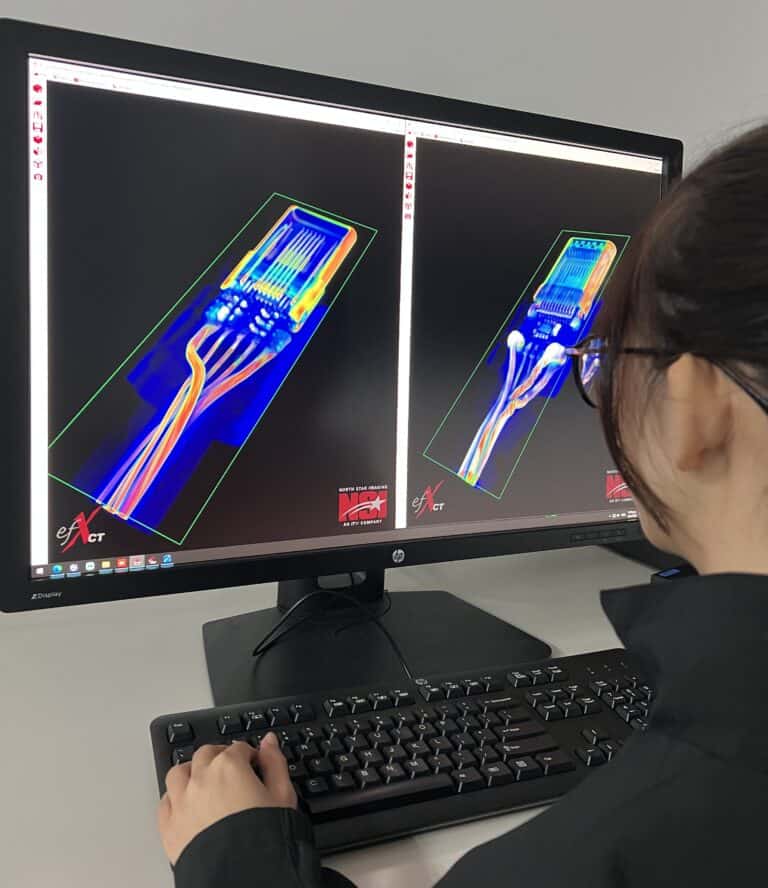
Using 3D X-ray computed tomography, laboratories can produce detailed internal images of USB-C cables without cutting them open, revealing the construction differences between a budget cable and a premium one. In this blog, we’ll examine what those X-ray images show, how CT scanning works, and why the technology matters well beyond consumer cables.
Why USB-C Cables Fail or Break: It's What's Inside
Cable failure rarely comes down to rough handling alone. More often, it traces back to shortcuts in internal construction that were present from the moment the cable left the factory. The most common failure points include:
- Poor solder joints at the connector. If the solder coverage is thin or inconsistent, the electrical connection degrades with each bend and plug cycle.
- Thin or inconsistent copper wiring. Some budget cables use fewer copper strands or substitute aluminium, limiting both power delivery capacity and data transfer speed.
- Weak or missing strain relief. The junction where the cable meets the connector absorbs the most mechanical stress. Cheap cables often have hollow or flimsy strain relief that can’t handle repeated bending.
- No shielding. Without proper electromagnetic shielding, signal integrity degrades faster, and the cable becomes more susceptible to interference.
None of these issues is visible during a visual inspection. Two cables sitting side by side on a shelf can appear nearly identical, yet one might last six months while the other holds up for years. That hidden gap in build quality is why USB-C cables stop working in ways that seem random but are actually predictable once you can see inside them.
X-Ray Imaging: Seeing What the Eye Can't
In a 2023 study, CT-scanning firm Lumafield compared several USB-C cables ranging from around $4 to Apple’s $129 Thunderbolt 4 Pro cable. The results illustrate exactly what a USB-C cable internal structure X-ray comparison can reveal about build-quality differences that would otherwise remain hidden.
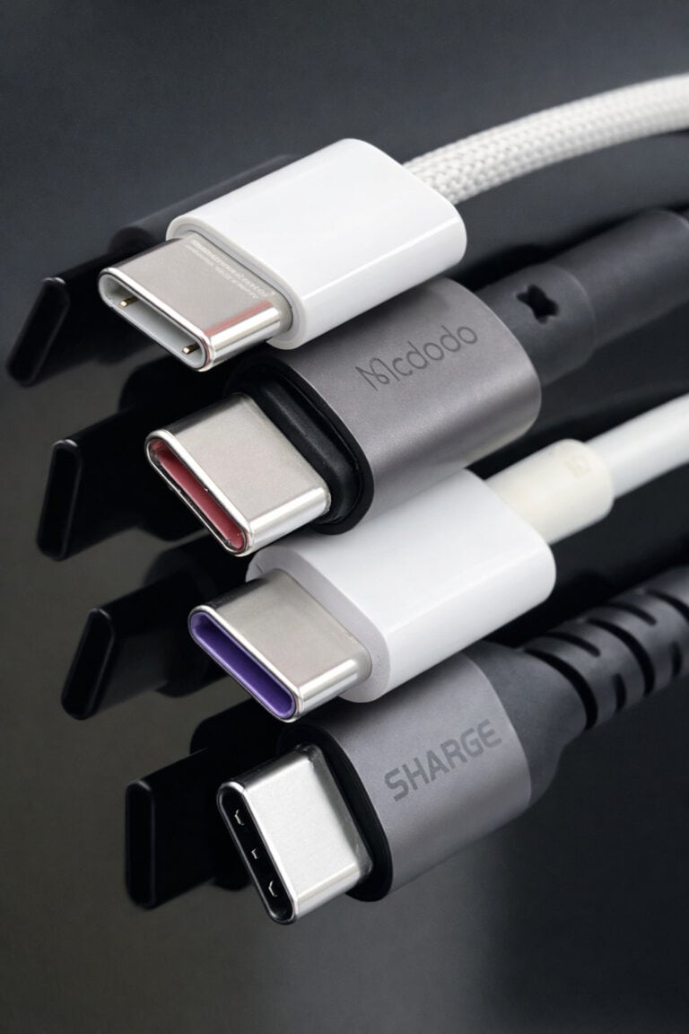
In 2026, we at PTS conducted our own studies on USB-C cables, performing CT scans on USB-C-to-USB-C cables from Apple, Sharge, Mcdodo, and a generic third-party brand. Comparatively, Apple and Sharge’s cables were priced higher as premium options, followed by Mcdodo as a mid-range cable, and the generic cable was the most affordable.
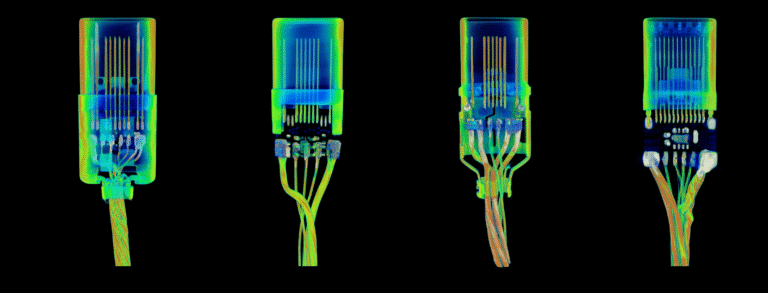
Connector Build
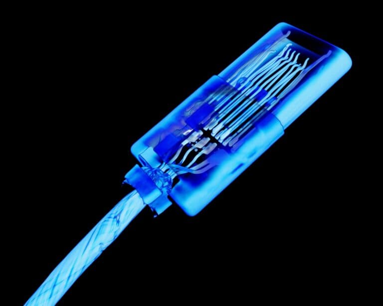
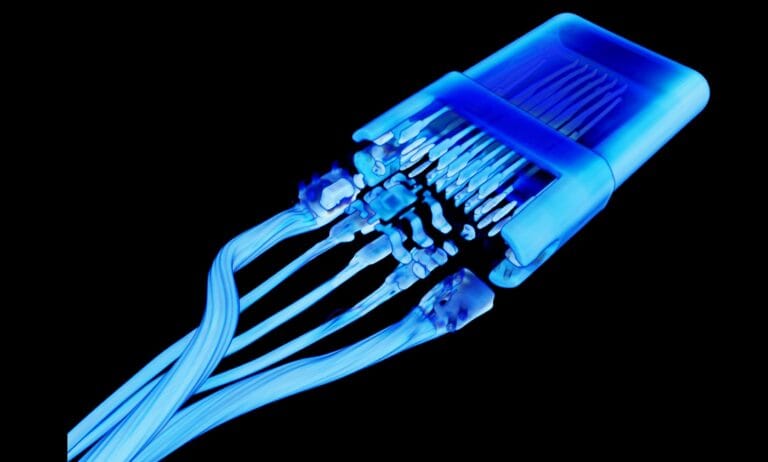
The budget cable showed connector pins and shells floating independently within an over-moulded plastic housing, with no dedicated circuit board and no structural bonding. Wires were soldered directly to the pins with minimal coverage.
The Apple cable, by comparison, featured a 10-layer printed circuit board assembly (PCBA) with all 24 pins mounted independently and properly routed through the board. That level of engineering is immediately apparent in a USB-C X-ray comparison but completely invisible from the outside.
Internal Wiring
Lumafield’s scan of the cheap cable revealed just four active pins connected to thin wires, capping real-world data transfer at around 480 Mbps despite the product listing’s advertised 10 Gbps. Apple’s Thunderbolt 4 cable contained 20 separate wires, 10 of which were coaxially shielded and individually soldered to the PCBA.
In our scan of Mcdodo’s and Sharge’s USB-C cables, we observed electronic marker (e-mark) chips in the wiring, enabling greater power delivery and higher-wattage support for faster charging. The cables were also thicker.
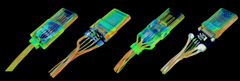
Strain Relief
This is the area where most cables ultimately fail: the neck where the cable meets the connector. In the cheap cable scans, strain relief was either minimal or absent. Apple’s cable featured a single-piece strain-relief fitting crimped from eight directions, engineered to distribute bending stress across the junction evenly within a seamless, unibody design.
Our scan of Mcdodo’s cable found that it had neither intrinsic strain relief nor a unibody design. Instead, strain relief depended on overmolded plastic to hold the cables in place.
Understanding CT Scanning: How It Works
What Is CT Scanning?
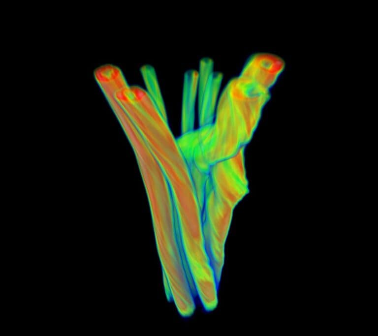
Computed tomography (CT) is a non-destructive imaging method that produces a complete 3D representation of an object’s internal structure. The process involves capturing hundreds of X-ray images at different angles as the object rotates on a stage, then using reconstruction software to assemble the 2D projections into a 3D volumetric model.
Unlike a standard X-ray, which produces a single flat image where internal features can overlap and obscure each other, 3D X-ray computed tomography allows engineers to slice through any plane, isolate individual layers, and examine specific features at high magnification. There’s a substantial difference, as 2D imaging only shows a superimposed image of multiple layers onto a single plane, whereas CT provides a fully navigable internal map in the form of 3D volumetric data.
Why It’s Suited for Product Analysis
CT scanning reveals hidden features without requiring disassembly, capturing solder joints, internal wiring, air gaps, and material density variations in a single scan session. Because the product remains intact throughout, the results reflect actual assembled conditions rather than a post-teardown state in which components may have shifted.
High-resolution scans capture micro-level detail that even 2D digital radiography would miss. This resolution is critical for gathering meaningful data, especially for smaller products like a USB-C connector, where tiny pins, fine wires, and shielding layers are packed into a minuscule space.
From Image to Insight
The 3D model created from CT data can also be measured against CAD files for dimensional deviation analysis, inspected for defect types like porosity or voids, and used to pinpoint exact failure locations within a component. Rather than confirming that something went wrong, it identifies precisely where and, in many cases, why.
This same technology is what 3D scanning services Singapore laboratories use for X-ray comparisons of USB-C cable internal structures, as well as broader electronics inspection, failure analysis, and reverse engineering across multiple industries.
Why This Matters: Real-World Applications
For everyday consumers, CT scans serve as useful validation that premium pricing can reflect genuinely superior construction. It’s a practical reference point when evaluating cable purchases.
The greater commercial value of CT scanning, however, sits with engineering teams, product designers, and quality assurance professionals who need verifiable data on internal build quality.
For Engineers & Designers
- Identifies weak points in prototypes before committing to full-scale production, including strain relief, solder coverage, and material voids.
- Compares supplier components based on actual internal construction.
- Catches failure-prone design areas early and iterates before they become warranty or field-failure issues.
For QA & Failure Analysis
- Determines exactly where and why a product failed without destructive teardown or guesswork.
- Verifies batch consistency across production runs without sacrificing samples.
- Builds a documented evidence base for root cause investigations and supplier audits.
The Commercial Angle
Stronger internal build quality directly translates into longer product lifespans, lower return rates, and reduced warranty costs. CT scan data also supports premium product positioning with measurable evidence, enabling manufacturers to substantiate quality claims with imaging evidence rather than marketing language alone.
Get the Full Picture with PTS's CT Scanning Services
While there are price differences among USB-C cables, they reflect real, measurable differences in internal construction, from wiring and solder quality to shielding and strain-relief design. X-ray CT scanning makes these differences visible, quantifiable, and actionable for engineering and quality teams.
As an independent test laboratory operating since 1985, Professional Testing Services, an ISO/IEC 17025:2017-accredited laboratory, offers USB-C X-ray comparison capabilities alongside a full suite of 3D scanning services in Singapore and X-ray inspection for electronic components via digital radiography solutions. With our facilities in Singapore, Malaysia, Indonesia, and Brunei, we support manufacturers, OEMs, and engineering teams across the region with fast, reliable, and accurate non-destructive testing.
Choosing the Right Test for Your Situation
- Material grade verification or warehouse sorting: PMI (primary method)
- Surface contamination check on stainless steel: Ferroxyl test or copper sulphate test
- Quick field sorting without equipment: Spark test (preliminary only)
- Complete QA for critical components: PMI for material verification, combined with ferroxyl or copper sulphate testing for surface contamination
A layered approach works best for operations handling both carbon steel and stainless steel. PMI confirms the material is correct upon receipt or before fabrication, followed by a full QA to verify surface integrity after processing, giving full coverage from incoming material through to finished component.
Frequently Asked Questions About USB-C Cable X-Ray Inspection
Most failures trace back to internal construction shortcuts: thin copper wiring (or aluminium substitutes), poor solder coverage at the connector pins, minimal or absent shielding, and weak strain relief at the cable-connector junction. These flaws accelerate wear and signal degradation even under normal use conditions. Because these issues aren’t visible externally, two cables that look identical can have vastly different functional lifespans.
A 2D X-ray (digital radiography) produces a single flat image, which is effective for spotting major defects but limited when internal features overlap. 3D CT scanning captures thousands of X-ray projections from different angles and reconstructs them into a volumetric model. This way, you can slice through any plane, inspect individual solder joints, and measure internal features without physical disassembly.
No. CT scanning is entirely non-destructive, and the cable or component remains fully intact throughout the scanning process. This is one of its primary advantages: the scan reflects real-world assembled conditions rather than a teardown sample that may have been altered during disassembly. This is extremely important for failure analysis, where the unit under study is unique and critical and must be handled with the utmost care before any physical manipulation or further investigation.
Accordion Content
Industrial CT scanning is used across a wide range of sectors and applications, including castings, welds, 3D-printed parts, mechanical assemblies, medical devices, and automotive components. Any scenario that requires inspection of internal features, defect detection, or comparison against CAD models without physical disassembly can benefit strongly from CT scanning.
Talk to us today
Contact PTS today to schedule a consultation for how we can help you with CT scanning. We also offer a complimentary first CT scan for new customers to give you an insightful look into this technology.


